
SIEMENS EDA FORUM 2024 即將於8月20日隆重登場!
近年全球 AI 浪潮迅速崛起,電子行業的數位轉型已成為當務之急,IC和系統設計產業將加速創新,迎來新的里程碑。
亮點搶先看:
產業趨勢:搶得先機聆聽大咖點出半導體方向。
深入技術內容:分享最新的IC設計驗證技術。
專家交流:與西門子的專家以及其他行業菁英進行面對面的交流。
新觀點和最佳實踐:從西門子的客戶那裡獲得寶貴的經驗和見解。
六大主題不容錯過:
#AI-infused IC EDA #Automotive IC #Design for Power #Advanced Mega Chip #3D IC #Custom IC Design
邀請您即刻報名與會,共同掌握產業的新契機,開創IC設計驗證的新方向。
Exploding societal demand for semiconductor-enabled products means that semiconductors are now a central part of the worldwide geopolitical discussion. With semiconductors now driving core product differentiation in virtually all areas, broad availability of high-quality leading-edge semiconductor processes and an advanced heterogeneous packaging ecosystem is critical to your success. Let’s explore how Siemens are delivering advanced manufacturing, AI enhanced design automation tooling, and open ecosystem enablement – to enable your next generation of designs.

CEO, Siemens EDA Silicon Systems
Mike Ellow is CEO, Siemens EDA Silicon Systems, Siemens Digital Industry Software, a business unit of Siemens Digital Industries. He leads Siemens EDA (formerly Mentor Graphics) Integrated Circuit Solutions (ICS) R&D, as well as EDA Global Sales. Ellow has led Siemens EDA Sales since August 2014 and Siemens EDA ICS R&D since 2023. He brings 30 years of executive sales and technical management experience, along with a proven track record of building strong sales and engineering teams while delivering positive, predictable results. These results are built on a foundation of focusing on customer success.
Ellow joined Mentor Graphics in March 2014 as part of the company’s acquisition of Berkeley Design Automation, where he was Vice President of Worldwide Sales. Prior to that, he held various positions at Cadence Design Systems, overseeing sales in North America, Europe, and India, culminating in the role of Corporate Vice President, North American Sales. Prior to Cadence, he held management, marketing, and engineering positions in a number of different industries. He started his career as an electrical engineer at Hughes Aircraft.
Ellow has a BSEE from Lehigh University, an MSEE from the University of Southern California, and an MBA from California State University, Fullerton.
AI and software-defined systems have become essential to various industries, transforming the way we operate. TSMC is leading the way in developing leading technology and advance packaging technology. Along with our OIP partners, we have built a comprehensive ecosystem and innovated solution to enable our customer’s innovations. These changes have given rise to a new era in semiconductors, with an exciting future. In this keynote, Dan will delve into the opportunities and possibilities that TSMC has experienced, the challenges that it is currently facing and resolving, and how your involvement can bring power to the semiconductor industry to create a new era together.
Head of Ecosystem and Alliance Management Division, TSMC
Dan joined TSMC in 2007. He currently leads TSMC Ecosystem Partners program including EDA Alliance, IP Alliance, DCA Alliance, Cloud Alliance, and 3DFabric Alliance as part of company’s Open Innovation Platform® (OIP). OIP initiative is a comprehensive design technology infrastructure program enabling collaborations, innovations to reduce design barriers and improve first time silicon success. Prior to his current role heading up the design infrastructure management division, Dan led the Japan customer strategy team, the technical marketing and support team for the EMEA region in Amsterdam and was a part of the team leading the formation of Open Innovation Platform® (OIP), IP Alliance program. Prior to TSMC, Dan worked at Chartered Semiconductor both in the US and Singapore where he held a number of management positions, including Director of Platform Alliance, Director of eBusiness, Director of Design Services, and Director of Americas Marketing. He also worked at Aspec Technology and LSI Logic. Dan holds a Bachelor of Science degree in Electrical Engineering from UC Santa Barbara, a Master of Science in Computer Engineering, and an MBA from Santa Clara University.
GenAI triggered a lot of excitement and attentions to semiconductor sector and IC design. Being the front and center to "enable" GenAI across the board, how will GenAI change our operating model in IC design? How would that shift our skill and expertise requirements? How best to adapt to the change that's coming along the way? BCG, as a long term partner to Semiconductor Industry Association to lead industry wide analysis, will come and share the latest perspectives.

Managing Director and Partner Greater China, BCG
Mei Jung is the leader to Digital Operation practice in BCG Greater China, focusing on end to end operation transformation with AI implementation. Her industry experience covers across high tech (semiconductor, consumer electronics and etc.) and its adjacencies.
Relevant consulting experienceHow AI is changing every aspect of EDA

Senior Director of Engineering, Siemens EDA
Jeff Dyck is a Senior Director of Engineering at Siemens EDA, responsible for R&D for four software product lines in the Custom IC Verification (CICV) division, as well as the EDAi team. Prior to joining Siemens, Jeff was VP of Engineering at Solido Design Automation, where he led Solido's R&D teams, managed Solido’s product lines, and co-invented Solido’s AI technologies. Solido was acquired by Siemens in 2017. Jeff is now working on evolving the AI technology in Solido's products and beyond, as well as developing new disruptively differentiated AI accelerated tools.
Introducing Smart Verification: Unleashing the Potential of AI Within Functional Verification
Product Manager, Siemens EDA
Darron May is a Product Manager specializing in architecting Verification Management, Debug, and Coverage solutions. He recently spearheaded the launch of Verification IQ, our new collaborative data-driven verification solution, and is now driving the integration of AI/ML into our functional verification portfolio. He has over three decades of experience in the electronics industry, encompassing board, FPGA, and chip design and verification, as well as pre- and post-sales support, applications, consulting, and technical marketing. Prior to his tenure at Mentor/Siemens, he held engineering and applications positions in the Datacoms and EDA industries.

Senior Support Engineer, Siemens EDA
Layra has a decade of experience in IC design industry, technology expertise in mobile communications, digital and analog co-simulation, and UVM. She is responsible for overall technology of functional verification solution. She participates engagements with partners, joints customer initiatives, and takes a major role in the deployment of the major accounts such as MediaTek and ARM-China. She also develops and delivers technical training on SystemVerilog, QuestaSim, and Visualizer Debug Tool.

Senior Technical Manager, MediaTek Inc
Chienlin is a digital designer and integrator at Mediatek. Responsible for WIFI Baseband processor IP. Has 14 years’ experience in digital design. Has held position as integrator, IP designer, subsys platform architect designers and verification. Currently, focus on create new or refine methodology to improve design architect, verification and integration quality at Mediatek connectivity IP.
How do all the Calibre Interface solutions, including ones using AI, can speed your overall PV Closure Time

Senior Application Engineer Consultant, Siemens EDA
Jeffery has been a part of Siemens EDA for many years, bringing a wealth of experience in the EDA industry. He excels in Calibre physical verification, design optimization, and flow integration. Jeffery is dedicated to helping customers enhance performance, provide technical support, and improve the efficiency of Calibre products, ensuring smooth and successful tape-outs.
Aprisa 2.0 - Full RTL2GDSII Solution with AI Functionality

Chief Technologist, Siemens EDA
Alpesh is Chief Technologist at Siemens EDA, responsible for defining place and route tool solutions for sub-5nm technology nodes and deployment of Aprisa place and route solutions at leading semiconductor design companies. Prior to Siemens, he was Vice President of Applications Engineering at Avatar Integrated Systems and also worked in various Applications Engineering roles at Atoptech and Synopsys. He has 24 years of physical design experience supporting various EDA tools for numerous semiconductor companies. Alpesh’s area of expertise includes low power design and has few publications in that domain. Alpesh holds a Masters degree in Electronics Design and Technology from the prestigious Indian Institute of Science, Bangalore.
Accelerating high-sigma SPICE verification and library characterization with production-proven AI from Solido

Product Manager, Siemens EDA
Mohamed Atoua is a Product Manager for Solido Design Environment at Siemens EDA with more than 7 years of experience in the EDA industry. With a track record of blending technical solutions with business acumen, his current mission is to help circuit designers address the challenges of meeting higher design complexity faster with less effort through Siemens’ Solido Design Environment software.
His journey began at Cairo University, where he earned a bachelor's degree in electrical engineering, specializing in electronics with a minor in computer engineering. Atoua is currently pursuing his master's degree in business administration at the University of Illinois Urbana-Champaign, he thrives at the intersection of technology and management.
Principal MTS, Rivos, Inc
Delbert Liao is a Principal MTS at Rivos, Inc., responsible for custom IP design and third-party IP integration. He has 15 years of experience in the semiconductor industry. Before joining Rivos in May 2022, he spent nearly ten years at Augentix and MediaTek, focusing on analog design, SI/PI, and packaging design. Delbert holds a master's degree from National Tsing Hua University, Taiwan.
Automotive Test & System Life-Cycle Management
Application Engineer Manager - Tessent, Siemens EDA
Jeff Fan (范熾東) is Taiwan and ASEAN (台灣及亞太區) Application Engineer Manager for the Tessent product family at Siemens EDA. Jeff has over 20 years of experience in various DFT aspects with respect to hierarchical flows and architectures including Scan, Memory / Logic BIST, Diagnosis. Jeff has been Tessent support engineer for more than 12 years and lots of support experience in different kind of DFT designs.
Jeff has also worked with factory and worked together with development to develop Tessent multi-die solution. He has lots of insight knowledge about tessent 3D IC solution. Jeff holds a Master of Science degree in Electrical Engineering.
Shift-left SDV design with Siemens PAVE360 automotive digital twin solution

VP Hybrid and Virtual Systems, Siemens EDA
With over 25 years of experience in the Semiconductor industry having held senior technical roles at NVidia, Qualcomm, Texas Instruments, and others, Mr. Fritz is the Vice President of Hybrid and Virtual Systems leading the global autonomous IC and validation initiative at Siemens EDA. Mr. Fritz brings innovation of fast moving Silicon Valley companies to the Siemens EDA team by applying transformative technologies to the challenges of autonomous and connected vehicles.

Senior Manager, Automotive Go-To-Market APAC, Arm
With over 20 years in the high-tech industry, Jason Lee's diverse career spans engineering, product marketing, sales, and business development. Currently focusing on the automotive semiconductor market, Jason is passionate about driving the evolution of the software-defined vehicle, leveraging his extensive expertise to enhance Arm automotive solutions, shaping the future of automotive technology.

Senior Engineer, SiliconAuto
Jenny Huang works as a virtual prototyping expert at SiliconAuto. Currently, she is responsible for delivering solutions to address software early-stage development, PPA and E/EA definition challenges at different abstraction levels for virtual MCU/ECU platforms and digital twins in the automotive industry.
mPower at Ekepower: First class EMIR analysis for improving design productivity
mPower Power Integrity offers both transistor level and gate-level solutions. The transistor-level flow enables rigorous analysis of large-scale analog designs that were not possible before. This new capability allows design teams to replace expensive, engineering-intensive workarounds with consistent, repeatable analyses that enable confident tape-outs. The gate-level flow is a comprehensive solution for full-chip, cell-based power grid analysis and verification, including static and dynamic power integrity and reliability checking features that can be leveraged from the early design implementation stage to final sign-off.

Senior Application Engineer, Siemens EDA
Alvin Liu has joined Siemens EDA since obtaining a Master's degree in Electrical & Computer Engineering from the University of Arizona in 2015. He currently serves as a Senior Application Engineer responsible for Calibre products in Taiwan and Asean. Alvin primarily focuses on providing technical support and conducting product evaluations for Calibre LVS/PERC and mPower Analog & Digital in MediaTek Group.

Co-founder, EKEPOWER CORPORATION
Dr. Hsu has 20-year CMOS analog circuit design experience and 10-year EDA system integration experience. Besides CMOS integrated circuit design, Dr. Hsu also has much MEMS and heterogeneous integration experience, and his PhD. research is semi-passive smart contact lens platform for eye disease diagnosis.
Appying best practices to eliminate wasted power and achieving fastest time to ideal power
Designers face enormous challenges for low-power designs. Whether it is IoT at the edge, AI in the datacenter, robotics or ADAS, the demand for increased functionality in SoCs is rapidly outpacing the power budget. Power must be considered at every stage of chip design including performance, reliability and packaging. Waiting to address power until late in the design cycle – post-netlist or during physical implementation – can be extremely costly. The design may overrun the power budget, overheat, or have long term reliability issues that cannot be addressed at the gate level, layout or package selection. The best point in the design cycle to address power is at the beginning during the architectural and RTL stages. The earlier power analysis and optimization starts, the more likely a chip will meet its power objectives.

Principal Product Engineer, Siemens EDA
Mohammed Fahad works with Siemens EDA as Product Application Engineer. Fahad has 20 years of work experience in the field of Low Power, CDC and FPGA based system design. At Siemens EDA, Fahad is responsible for Low Power technology deployment and proliferation activities across a variety of Semiconductor customer base.
Understanding Power and Dynamic IR Drop for DFT Patterns Pre-Silicon Using Veloce
Power management of DFT patterns is a significant problem driven by the high density of chips, the slowdown of VDD shrinkage with advancing technology nodes, and the high activity of DFT patterns. Commonly, DFT patterns fail on the tester due to power-related issues and dynamic IR drop challenges. This session addresses the power implications and dynamic IR drop effects associated with Design for Test (DFT) patterns using Veloce, the leading hardware assisted verification platform. DFT patterns typically create 3 to 4 times more activity compared to functional patterns, yet the power delivery network is primarily designed to support functional patterns. This discrepancy often leads to test failures on the tester, necessitating modifications to ensure tests pass.
By leveraging Veloce's capabilities, we conduct comprehensive pre-silicon analyses to evaluate the power consumption and IR drop characteristics induced by various DFT patte rns. We demonstrate the importance of early detection and mitigation of power-related issues, presenting methodologies to identify and remedy DFT patterns for power efficiency and IR drop reduction pre-silicon. The Veloce DFT app allows for running DFT patterns thousands of times faster than traditional simulation. The Veloce Power App and Veloce IR Drop tool perform detailed analyses using Liberty, activity, and SPEF files to provide accurate and insightful information for DFT patterns. This solution offers a valuable framework for DFT and test engineers to enhance pre-silicon verification processes, ensure reliable DFT patterns, and reduce test time.

Applications Engineering Consultant, Siemens EDA
CY Chang is an Formal verification solutions AE at Siemens EDA. based in Taiwan. CY has more than 15 years of experience in
the semiconductor industry which including 10 years in EDA field and 5 digital designer role,CY joined Siemens in 2022 as part of the Onespin team.
Accelerate Time To Market With Latest Calibre MTFlex Solution
To meet market demands, IC chips must minimize their footprint and power consumption while adding functionalities and ensuring instant delivery to meet market needs. Therefore, heading to advanced nodes is essential.
Upon transitioning to advanced processes, the number of components per unit area and the checking items significantly increase, resulting long backend verification time.
To address these challenges, Siemens provides an optimal solution using MTFlex technology to significantly reduce backend verification Turn-Around-Time (TAT). This helps customers accelerate backend verification time for smooth tape-out and instant product delivery, seizing more market opportunities!
Large scale of data can be processed by Calibre parallelly throughout all connected cores in order to achieve a shortened total turnaround time.

Senior Application Engineer, Siemens EDA
Xiang Fang joined Siemens EDA as an application engineer in 2015. He is experienced in foundry tape-out flow optimization for years. Xiang currently focuses on helping customer to optimize the performance of Calibre products family.
Assistant Technical Manager, Novatek Microelectronics
GuoSheng Hong joined Novatek in 2018, he focused on backend verification flows from 40nm to advanced nodes ever since and witnessed how backend verification became more and more complicated.
Avery Verification IP delivers Accelerated Confidence from multi-die chip to datacenter software – UCIe, PCIe, CXL, VICS
Architects of today’s complex compute systems can design using a rich amount of new technology. At chip-level, 3DIC packaging breaking Moore’s Law, using the new UCIe protocol for D2D interconnect and creating a Chiplet economy. At board-level - PCI Express Gen 7 (PCIe7) with fast and wide mixed signal interfaces, breaking speed limits while ensuring integrity and security, and enabling CXL3.1 layered protocol for scalable CPUs, composable memory and specialized AI/ML coprocessors. And finally, completing the system with Software layers around all that hardware - which with our VICS products we can now verify Software alongside our RTL Hardware VIPs, in simulation and in emulation. Avery VIP provides verification solutions for all that hardware and software and delivers Accelerated Confidence to your team.

Application Support Engineer, Siemens EDA
Jimmy is a Technical Support Engineer responsible for front-end design and verification in the Asia-Pacific region. His main responsibilities include simulation verification and formal verification, as well as the development of new AI/ML based verification technology. He is dedicated to assisting clients in resolving various challenges they encounter during the design and verification process and providing efficient technical support to ensure their designs can smoothly pass verification and achieve the desired outcomes.
Streaming Scan Network (SSN) Update, customer experience sharing and advanced topic on ATE
In this session we will start with SSN advanced features update, such as fast IO support and flatten SSN design and then Novatek will share their experience on using SSN.
Advantest will give update SSN test advantage and shared what they have learned from SSN customer.
SSN flow can work from RTL, in 2023 November, Tessent introduce RTL Pro allow customers to check customer RTL design’s testability. This reduces design turn-around-time and improves time-to-market by allowing early identification and correction of testability issues.

AE Consultant, Siemens EDA
Ivan Chou is Siemens EDA field application engineer Consultant, focusing on Tessent Automotive solutions. Before joining Siemens EDA, he was a DFT assistant technical manager in Mediatek and a senior engineer in tsmc. He engaged the solution for yield enhancement and silicon diagnosis analysis for nearly ten years. He graduated from National Central University with both bachelor's degree and master degree in electrical engineering.

Technical Assistant Manager, Design for Testability, Novatek Microelectronics
16 years experience in DFT design field
Director, Performance Digital AE Dept., Advantest Corporation
Summer Chen is an AI/HPC application testing director in the V93000 Performance Digital business segment (AI/HPC, Mobile APU, ADAS, …). He is based in Advantest Taiwan Office and main role is to lead application team to service back-end team of local design company, OSATs and foundry for testing solution implementation, test program development and production problem solving. He holds a Master Degree in Electronics Engineering from Chung Yuan Christian University and has 20+ years of experience in the semiconductor industry.
Innovator3D IC - Comprehensive multiphysics cockpit for 3D IC Design
In this talk, we will explore the use of newly evolved planning and design tool, Innovator3D IC for the initial planning stages of 3DIC development. These advanced tools serve as the cockpit for embarking on 3DIC design, offering tailored functionalities to meet the diverse requirements of various applications. Additionally, they act as a crucial hub, connecting and integrating various verification and design tools, including multi-physics reliability verification, to streamline the entire development process.

Application Engineer, Siemens EDA
Tony Lin is responsible for Xpedition IC packaging software and 3DSTACK. Support customers in establishing 2.5D/3D IC verification processes, as well as solutions for High-Density Advanced Packaging (HDAP) and physical layout of package substrates.
Using Calibre 3DThermal to address thermal effects in 3DIC
Siemens Digital Industries Software introduced Calibre® 3DThermal, innovative software for thermal analysis, verification and debugging in 3D integrated circuits (3D-ICs). Calibre 3DThermal enables chip designers to rapidly model, visualize and mitigate thermal effects in their designs from early-stage chip and package-inward exploration through to design signoff by incorporating elements of Siemens’ Calibre verification software and Calibre® 3DSTACK software along with the company’s Simcenter™ Flotherm™ software solver engine. Calibre 3DThermal was developed to address challenges of 3D-IC architectures where controlling heat dissipation is a key requirement, considering metalization details and their impact on thermal considerations. This progressive approach enables designers to refine their analysis and apply fixes such as floorplanning changes and adding stacked vias or TSVs to avoid thermal hotspots and/or dissipate heat more effectively. This iterative process continues until the final assembly is complete, significantly reducing the risk of performance, reliability and manufacturing issues at final tape-out.

Foundry Lead, Siemens EDA
Alex Hung was mainly responsible for electronics cooling analysis with more than 10 years of experience in thermal simulation, covering data centers, computers, laptops, circuit boards and IC packages, etc. In recent years, he has served Siemens EDA as a senior product engineer, responsible for technical support and marketing of the thermal simulation verification process of IC design.
Senior Corporate Applications Engineer, Siemens EDA
Laura Tseng has over 10 years of experience in TSMC BEOL process development, with a primary focus on design rule development and layout auto-generation. She has also contributed to TSMC's 3DIC design flow development, where she was mainly responsible for 3DIC EDA thermal flow validation for 1.5 years. Currently, she is a Senior Corporate Applications Engineer at Siemens EDA, providing technical support for Calibre DRC, LVS, 3DStack, and 3DThermal solutions.
Design-for-test (DFT) technology scalable from 2D to 3D designs
As we delve into the critical role of Design-for-Test (DFT) in overcoming testing challenges in 2.5D and 3D designs, these designs present unique complexities stemming from heightened interconnect density and heterogeneous integration. In this talk, we will discuss how Tessent expands its leading DFT solution in 2D with a consistent methodology into the multi-die space. We’ll explore such tailored approaches for the prevailing new trend of multi-die integration technologies, alongside the ecosystem supporting them. Discover Tessent's cutting-edge solutions, including IEEE1838 compliant multi-die and IEEE1687 compliant IJTAG test access mechanisms, innovative hierarchical-DFT solutions like streaming scan network (SSN), and comprehensive fault coverage techniques for known good die (KGD) testing and die-to-die interconnect testing. By integrating DFT early in the design phase, Tessent streamlines defect detection reliably, reducing development time and costs and leading to the high yield.

Foundry Program Engineer, Siemens EDA
Jim Yang is the foundry program engineer for the Tessent product at Siemens EDA. Recently, he worked closely with foundry to develop design flow on hierarchical DFT, SSN and 3DIC test chip and accumulated lots practical experience on SSN and hierarchical DFT solution. Jim was a DFT engineer of design service company and solution engineer of EDA company before join Siemens EDA. Jim has many experiences on DFT aspect including MBIST, Scan, BSD and multi-die. He graduated from National Central University with degree in electrical engineering.
Innovative Approaches through xPD to Efficient 3D IC Package and Daisy Chain Design
We will delve into the utilization of advanced package layout tool, xPD to tackle the challenges encountered in advanced package. We will explore how xPD effectively and swiftly accomplish intricate daisy chain designs within advanced package. By showcasing the functionalities of xPD, we aim to demonstrate their efficiency in overcoming complexities and enhancing the overall design process.

AE Consultant, 3D-IC Packaging, Siemens EDA
JEddy Lu is in charge of HDAP (High Density Advanced Packaging) solutions in SEDA, including Innovator 3D IC, Xpedition Packaging tools and Calibre 3DSTACK. Eddy has supported customers for building up 2.5D/3DIC verification flows to verify system connectivity, and completing physical layout of advanced Fan-out RDL, interposer and Substrate designs.
HyperLynx Comprehensive Simulation of Substrate desing in Advance Package
As substrate design in advanced package becomes increasingly complex, the demand for more advanced system and verification tools is imperative. This includes the need for comprehensive validation of substrate designs in advanced package, which entails utilizing tools such as SI analysis, PI analysis, and DRC. We will introduce latest version HyperLynx with advanced function and GUI design to complete these simulation & check in ensuring the integrity and reliability of substrate designs, ultimately leading to the successful implementation of advanced packaging technologies.
Senior Application Engineer, Siemens EDA
Rita is currently a Senior Application Engineer at SiemensEDA. With over 10 years of experience in a renowned system manufacturer, she possesses extensive expertise in PCB-level simulation and verification. Rita also has practical experience in driving automation in PCB design.
After joining SiemensEDA, Rita has participated in the development of design processes for multiple system and semiconductor manufacturers. She has also assisted domestic and international clients in valuable experiences in signal reliability analysis, design, and verification.
Custom IC for a Connected World
Custom IC is the electronic interface connecting processor to the world. For example, you need to make a call and pick up your mobile phone, motion is detected, the screen comes on and the processor wakes up, you select the phone icon on the screen and the appropriate radio and antennas are enabled. All these steps are driven by custom IC’s. Siemens provides enterprise-ready, custom IC design flow for innovative designs supporting both FinFET and planar analog, analog mixed-signal. PDK support is available from the large to the small, specialized foundries. With over 30 years of experience and thousands of design tape outs, this platform is well suited for all types of custom designs, from analog, analog mixed signal, image sensors, memories, power transistors, MEMS and photonics.

Design Kit Development Manager, IC Design Solutions, Siemens EDA
Tony Liao is the Design Kit Development Manager of ICDS Foundry Enablement Group. He has been working in the foundry and EDA industry for 23 years. Before joining Siemens EDA, he was the manager responsible for PDK development and design flow automation at UMC. Tony holds both Master and Bachelor degrees in Electronics Engineering from National Chiao Tung University.
Supercharged high precision Custom IC Verification with AI-accelerated Solido Simulation Suite
Artificial Intelligence (AI) continues to revolutionize custom IC verification enabling massive runtime, scalability and usability benefits, resulting in more differentiated silicon designs. In this session we introduce Solido Simulation Suite and discuss how Solido’s new SPICE and FastSPICE technologies, including in-simulator AI, provide production-accurate results orders of magnitude faster than traditional methods. Attend and learn how to achieve faster and more accurate SPICE-level verification and analysis, across multiple process, voltage, and temperature (PVT) corners, and utilize this information to inform high-value design optimization steps.
Principal Product Manager, Siemens EDA
Pradeep Thiagarajan is a Principal Product Manager at Siemens EDA for Custom Simulation products, including SPICE, fast SPICE, and Mixed-signal technologies. He has over 23 years of experience in the Semiconductor industry spanning roles in Analog IP design, SoC program management, and EDA product management and marketing. He is currently translating his IC engineering experiences into the EDA software industry to further verification technology. He has an M.S. in Electrical Engineering from University of Minnesota and holds 41 US patents.
Trust but verify your design IP with Solido IP Validation
Design IP is a key component of silicon production flows. The production and integration of design IP helps facilitate reusability in design components and shorten production cycles, and has become an essential element in modern SoC design methodologies.
IP validation is a key factor in determining time-to-market and silicon success. Design IPs are encapsulated in multiple views and formats including logical, timing, physical, electrical views, as well as custom formats. It is crucial to identify potential errors and inconsistencies across these different views and formats early on, to avoid integration or design closure issues, which can often result in increased costs, tapeout schedule delays, or post-silicon ECOs.
Solido Crosscheck and IPdelta, part of Solido IP Validation, provide a complete QA framework for the validation of all IP, regardless of type or technology, covering all design views and formats used for IP production and integration workflows, as well as version-to-version IP QA.
In this session, we will discuss common IP issues discovered and how Solido Crosscheck and IPdelta help identify IP issues early in the design flow, ensuring quality and consistency of IP, speeding up design cycles, and enabling a high-quality IP release at every iteration.

Director of Product Management, Siemens EDA
Wei-Lii Tan is Director of Product Management in Siemens DISW’s Custom IC Verification division for Solido’s AI-enabled verification & characterization, and IP validation product lines. Wei-Lii has 16 years of experience in semiconductor and EDA, having worked on both digital and analog methodologies. He has a master’s degree in electrical engineering from Mississippi State University, and an M.B.A. from Santa Clara University.
Efficient automated simulation optimization solution for electrical and thermal integration in Power Module design
Introducing Siemens EDA's closed-loop product development platform from design to simulation to address the design challenges of electricity, heat and stress in power modules, which realizes automatic design optimization and greatly reduces prototyping and testing costs. This technology solution shortens time-to-market and improves the quality and reliability of power supply power modules in order to enhance the competitive ability of differentiation. Through the successful cases of domestic and international power module manufacturers, we will share with you the experience of how advanced enterprises use Siemens EDA power module solutions to significantly improve the efficiency of product development.

EBS PacRim AE Manager, Siemens EDA
David Xu is currently the Siemens EDA EBS PacRim Application Engineering Manager with over 20 years of industry experience. He is responsible for the technical solutions promotion and support for medium and large system customers in the PacRim region. David has extensive experience in electronic system packaging and board level design, simulation and data management. In recent years, he has been committed to promoting system solutions, system integration of thermal and electrical technology solutions, as well as the application and promotion of automated design and simulation processes.
Reduce design iteration time with Calibre “Shift-Left” solution – Realtime, DE, Recon
Leveraging the Calibre engine, DE rapidly enhance design quality, and Recon intelligently filter rule checks. Integrated with a RealTime interactive interface, users can receive verification results early, reducing the debug review cycle and enabling products to hit the market in a timely manner, gaining a competitive edge.

Senior Application Engineer, Siemens EDA
With over a decade of experience in Calibre software applications, combining practical expertise in advanced processes from both semiconductor foundries and IC design companies, Frances serves as a Senior Application Engineer at Siemens EDA. In this role, she is responsible for promoting Calibre-related products, providing technical support, and serving as a course instructor.

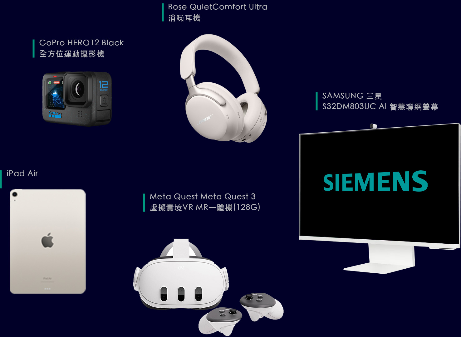
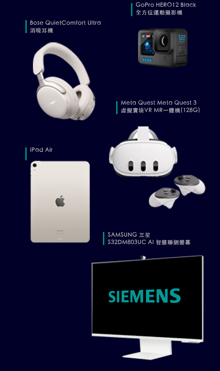
前50位完成報到者,可同步於報到時領取統一集團100元商品禮券。

14:30 -14:50 於現場攤位舉辦抽獎,投入名片一張就有機會獲得價值
美金1,250為期6個月的EDA on-demand training libraries Pass。
* for the existing customer only
如有論壇相關問題請與Siemens EDA forum 活動小組連繫: chester.kuan@anpencs.com